


The design of a printed circuit board (PCB) is one of the essential stages of electronic product development. There is no electronic product that would work without PCB, also known as the ‘brains’ of the device. This board connects electronic components with each other, thus, making your product work. PCBs can vary in size and complexity. First, your board should fit the size of your product. Second, PCB has layers the number of which depends on the complexity of your device.
Here is some general information about PCB design that will allow you to understand this process better.


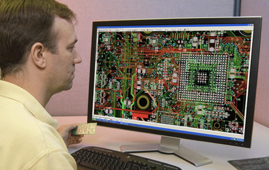
1. Schematic
PCB design begins with a schematic. In other words, a file with the description of all the components and connections of PCB. This description includes component specifications, their physical dimensions, placement, and other details. The schematic is created with the use of the software. Electronic design professionals use such software tools as Quadcept, Altium, PADs, and others. On the basis of the schematic, an actual PCB will be created.
2. Layout
The layout is the allocation of the components of PCB in accordance with the layers. The allocation is based on PCB sections distinguished by electronic designers regarding the functionality of the device. This process is more complex than the schematic since it places the actual components on the actual board. In addition, locating the components, electronic designers must keep in mind possible interference between components and avoid it when necessary. All the information about PCB components and their exact location on the board is then collected in a file that is further used in the manufacturing of PCB.
3. Printing out
After the schematic and layout creation, the circuit board is printed out. At first, it is unassembled. In other words, the board does not contain the components. They are added at the next stage of PCB design.
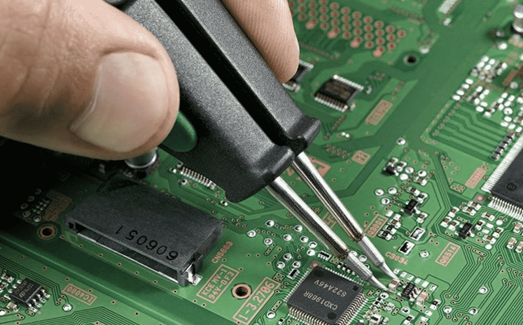
4. PCB assembling
After printing out the board, developers place the components on the board and, thus, PCB results in an assembled circuit board – PCBA. Keep in mind that in order to save time you should better order all the components in advance and ensure that all of them are in stock.
5. Testing
Finally, after all the components are placed on the PCB and permanently connected to the board and each other, developers test the assembled board for quality. It is a very important stage of PCB design. Testing allows identifying whether the components are connected to each other and whether everything works as planned. This stage includes different tests, such as ICT (In-circuit test), AOI (Automatic Optical Inspection), X-ray, and others.

As you see, the process of PCB design is complex and includes far more than simply printing the board and adding details. Indeed, working on PCB developers also manage supply chains and conduct various testing, not to mention the creation of the schematic. So, if you want to avoid all the problems linked to this process, consider hiring electronic design professionals. Having years of experience, they will easily design a PCB for your product.