Imagine a world where all our modern conveniences—smartphones, computers, even your coffee maker—didn’t function as they should. It might sound like a scene from a science fiction movie, but this could be our reality without the unsung hero of the electronic world: the printed circuit board (PCB). Creating these essential components through flex pcb fabrication is a cornerstone of nearly every device we use today. Let’s learn how to create printed circuit boards that power our daily lives.
What is PCB Fabrication?
PCB fabrication is the process used to manufacture PCBs, which provide the structural foundation to support and electrically connect electronic components through conductive pathways, pads, and other features etched from copper sheets laminated onto non-conductive substrates. This process involves multiple steps to ensure that the final product accurately meets specific functionality and reliability requirements of modern electronics, such as smartphones, computers, and medical devices.
Step 1: Design and Output
The journey of PCB fabrication begins in the design phase, where engineers use specialized software to meticulously lay out the circuit, ensuring all electrical paths are optimally mapped to meet the device’s unique specifications. Once the design is perfected, it is converted into a Gerber file, an open ASCII vector format for printed circuit board (PCB) designs that details every aspect of the board, from copper tracing to precise hole placement, ensuring a blueprint for accurate production.
Step 2: From Film to Board
In the next step of how to create printed circuit boards, the Gerber file is transferred to a protective mask on the copper boards using a photolithographic process. This involves exposing the board to UV light, which hardens a photoresist layer applied to the board. The board is then developed to remove unhardened photoresist, exposing the underlying copper that needs to be etched away.
Step 3: Etching the Copper
Following the design transfer, the exposed copper is chemically etched away, a critical phase in PCB fabrication. This is typically accomplished using a solution that selectively removes the excess copper, leaving behind the precise copper traces that define the circuit’s pathways. This step is crucial as it intricately shapes the connectivity and functionality of the circuit components within the board.
Step 4: Layering and Bonding
For more complex, multi-layer PCBs, this step involves layering and bonding multiple etched copper sheets together. Each layer, with its unique circuit design, is aligned and bonded using heat and adhesive to form a single, cohesive PCB. This process is essential for circuits in devices like motherboards, where multiple layers work harmoniously to support advanced functionalities.
Step 5: Drilling and Plating
Once the layers are securely bonded, holes are drilled to accommodate vias, which are essential conductive pathways connecting different PCB layers. These holes are then plated with copper, establishing robust electrical connections across the board’s layers. This step is a critical component of the entire PCB fabrication, ensuring multi-layer integration and functionality.
Step 6: Solder Mask Application
The next step involves applying a solder mask over the entire surface of the PCB, excluding the pads where electronic components will be soldered. This mask is vital as it protects the delicate copper traces underneath from accidental electrical shorts and physical damage. It also gives the PCB its characteristic green color, though other colors can be used based on personal preferences.
Step 7: Silkscreening
Silkscreening adds the final visual elements to the PCB, which involves printing critical information, such as component labels and test points, directly onto the PCB surface. This includes where parts should go and where connections happen. It’s super useful for the people who build and repair these boards. They can see exactly where everything fits, making assembly and future fixes much easier and ensuring everything is straightforward, helping technicians do their job without guesswork.
Step 8: Testing and Quality Assurance
The final step in how to create printed circuit boards is a comprehensive testing phase. Each PCB is rigorously tested to ensure it functions according to its design specifications. This quality assurance process checks for any potential defects and ensures that the PCB will reliably perform its intended function in real-world applications, maintaining the integrity and safety of the electronic device.
Once packaged and dispatched, the PCBs reach their final destination, where they are integrated into various electronic devices. This easy integration step is pivotal as it involves assembling the PCBs with other components like processors, memory, and sensors, bringing the whole system to life.
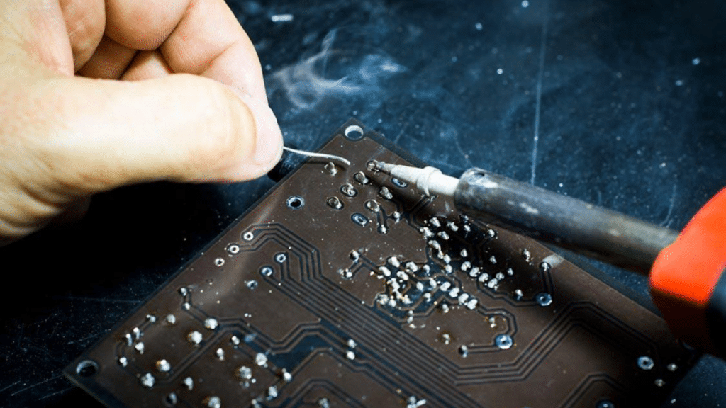
Technicians mount and solder components onto the HDI PCB, ensuring each piece fits and functions as intended. This critical assembly process transforms the bare boards into the operational heart of electronic devices, ready for use in everything from consumer gadgets to critical medical equipment.
In conclusion, PCB fabrication is a process that turns theoretical circuit designs into functioning electronics. From the initial design phase to the final quality assurance tests, every step is crucial in shaping the technologies that make our modern life possible. Whether you are a budding engineer or a curious enthusiast, understanding how to create printed circuit boards not only demystifies a part of the electronic products around us but also appreciates the incredible technology behind them.
